TK-LND915F LoRaWAN US915 Evaluation Kit
Quick Start Guide — for Development, Testing and Prototyping (EN, V1.1)
Revision History
| Version | Date | Author | Description |
|---|---|---|---|
| 1.0 | 2026/09/28 | — | Initial version, prepared based on the AT Command Standard Manual Rev 1.6 and the DTU Quick Start Guide. |
| 1.1 | 2026/10/13 | — | Added Chapter 11 FCC compliance statement (EN edition). |
1. TK-LND915F Hardware Introduction
1.1 Overview
This product is the TK-LND915F evaluation kit, built in a core-module-plus-baseboard architecture with rich interfaces. It is mainly used for module function verification, RF performance testing, peripheral interface debugging, and product prototype development. The kit integrates a complete power conversion circuit, an RF antenna connector, two independent TTL serial ports, a debug/download interface, user control buttons, and multiple general-purpose expansion headers, helping developers quickly complete chip function evaluation, AT command debugging, firmware flashing, sleep/wakeup, and other development tasks.
1.2 Core Module Introduction
| Item | Specification |
|---|---|
| Processor | 32-bit Arm® Cortex®-M4 CPU |
| Storage | 256KB embedded encrypted flash on chip; up to 64KB of on-chip SRAM divided into SRAM1 and SRAM2 |
| Network | LoRaWAN |
| Modulation | (G)FSK, (G)MSK, BPSK |
| USB Interface | Available for download and debugging |
1.3 Evaluation Kit Packing List
- One tested LND915F development board (core board + baseboard)
- One LoRaWAN high-frequency antenna
- One DC12V/2A power adapter
- Two USB-C data cables
- One USB-to-TTL adapter board
1.4 Development Board Layout and Interfaces
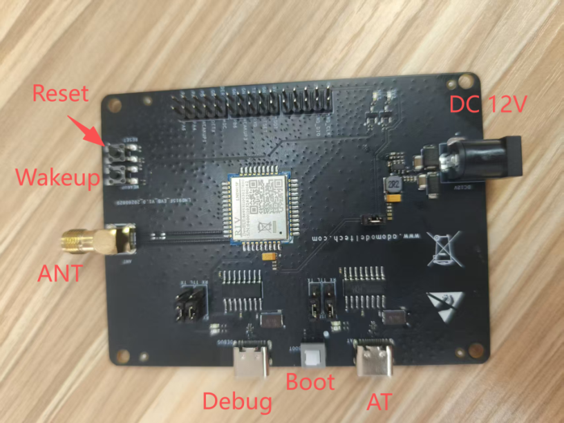
1.5 Main Hardware Description
1.5.1 Power Supply
The operating voltage of the TK-LND915F core board is 1.8-3.6 V (typ. 3.3 V). The development board provides two power supply options:
- DC12V jack: powered by the supplied DC12V/2A adapter or a battery. The board uses a JW5060T DC-DC converter to step the 12 V input down to 3.3 V.
- 3.3 V DC supply: the header at the bottom of the board provides a 3.3 V pin.
1.5.2 Buttons and Indicators
The TK-LND915F development board has three physical buttons:
- RESET - reset button
- WAKEUP - wake-up button
- BOOT - latching button that switches between download mode and normal operating mode
The board also has two status LEDs and two groups of serial-port LEDs:
- POWER LED - power status
- NET LED - network status
- Two groups of TXD/RXD serial-port LEDs
1.5.3 USB Interfaces
The TK-LND915F development board has two USB Type-C interfaces. Both are routed from two independent UART ports of the core module through TTL-to-USB chips. One is the AT command port, dedicated to sending AT commands for module configuration; it can also be used as a download port for firmware flashing. The other is the DEBUG port, used for system log output so developers can observe the module's internal running state.
1.5.4 Antenna Connector
The board provides one antenna connector, which is the RF transceiver port of the module. Connect an external antenna for wireless transmit/receive testing. Use it together with the supplied LoRaWAN high-frequency antenna.
1.5.5 Expansion Interfaces
The board provides three expansion headers, including SWD debug signals, multiple GPIOs, power, wakeup, and reset signals, allowing users to connect external peripherals for secondary development.
2. Hardware Environment Setup
2.1 Prerequisites
Before using this kit, prepare the required hardware and software environment. Hardware: the development board, a DC12V power adapter, and one of two serial-port options — Option 1: a USB-to-TTL serial module and Dupont wires; Option 2: a USB-C data cable. Also prepare the supplied antenna.
2.2 Hardware Connections
- Antenna connection
The ANT RF connector is the wireless transceiver port of the chip. Before powering on, firmly connect the supplied LoRaWAN high-frequency antenna to the ANT RF pad. - Serial port wiring (choose one of the two interaction methods via the onboard selector header)
The board has two TTL-level serial ports: the AT port and the DEBUG port. Both are 3.3 V TTL level.
Serial port selection logic:
A selector header with jumper caps switches the serial path. Only one method can be used at a time; do not connect both simultaneously to avoid signal conflicts.
Method 1: USB-to-TTL module. Use crossover wiring: connect the board's TX pin to the RX pin of the USB-to-TTL module, the board's RX pin to the module's TX pin, and connect the GND of the development board to the GND of the USB-to-TTL module to ensure a common ground.
Method 2: USB-C cable direct connection. Connect one end of a USB-C data cable to the board's USB-C connector and the other end to a PC USB port. Configure the onboard selector header in advance to switch to the USB-C path. The onboard serial chip provides USB-to-serial conversion, and the PC recognizes a virtual serial port — no external TTL module is required.
The AT port is used to send AT commands and configure module parameters, and also for firmware flashing; the DEBUG port prints module logs for troubleshooting. During development and debugging, it is recommended to connect both ports so you can view system logs while sending AT commands.
- Power connection
Connect the DC12V power adapter to the DC12V power input jack on the left side of the board. Before connecting power, verify that the adapter output is DC12V (12V/2A recommended) and that the polarity is correct. Do not reverse the polarity or apply overvoltage. The onboard power circuit converts the 12 V input to a 3.3 V VDD rail supplying the core module and onboard peripherals. Confirm all wiring is correct before applying power. - Function buttons and expansion header wiring
The onboard RESET and WAKEUP buttons can be pressed directly on the board. To control reset or wakeup externally, route the corresponding signal pins from the expansion headers at the bottom of the board and connect external control circuits with Dupont wires. The BOOT button at the top of the board switches the module boot mode between download mode and normal operation; hold it while powering on for firmware flashing. In normal operation it is not needed.
3. Quick Start Procedure
- Step 1 — Following the hardware setup chapter, select the serial interaction method, use the jumper caps to select the serial path, and connect the antenna, DC12V power, and serial equipment. Check all wiring and make sure there are no shorts or misconnections.
- Step 2 — Open a serial terminal tool on the PC and create two serial sessions (when both ports are used). Set the serial parameters to 9600 baud, 8 data bits, 1 stop bit, no parity. With the USB-C method, the PC automatically recognizes the virtual serial ports; with the USB-to-TTL module, make sure the module driver is installed.
- Step 3 — Connect the DC12V power to power on the module. For firmware download, press the BOOT button while powering on to enter firmware download mode; for normal debugging, do not press BOOT — the module enters normal operating mode directly after power-on. After power-on, check the DEBUG port for boot messages to confirm that the module started successfully.
- Step 4 — AT command interaction and debugging. Switch to the AT port window and send AT commands according to the supplied AT command document to configure module parameters, check the module status and sleep mode, etc., verifying the module's basic functions.
- Step 5 — Peripheral and low-power verification. Use the onboard WAKEUP button, or input a signal through the WAKEUP pin on the expansion header, to test the sleep/wakeup function; use the RESET button to test hardware reset; connect sensors or other peripherals to the GPIO pins at the bottom of the board for I/O function development and verification.
- Step 6 — Firmware upgrade. To update the chip firmware, press the BOOT button while the board is powered off, then power on the board — the chip enters download mode. On the PC, use a flashing tool to download the firmware via the SWD interface or the AT port. After flashing, power off, release the BOOT button, and restart the board to return to normal operating mode.
- Step 7 — Power consumption test. After flashing the corresponding firmware and configuring the sleep mode, disconnect all power sources and the jumper caps on the headers, supply power through the indicated header pins using a DC power supply, and measure the module's sleep power consumption.
4. Overview
4.1 Purpose
This document guides R&D and test engineers through the complete test procedure for LoRaWAN network joining, uplink data transmission, and downlink data reception of the TK-LND915F module (hereinafter "the F module").
4.2 Intended Audience
- R&D engineers
- Technical support engineers
- Test engineers
4.3 System Architecture
The system involved in F module joining and uplink/downlink testing is as follows:
The F module (TK-LND915F development board) acts as a LoRaWAN end node and communicates with the gateway over the LoRa wireless link. The gateway, acting as a data relay, forwards node data to the Network Server (NS). The NS handles join validation and uplink/downlink data management. During testing, AT commands are sent to the F module from a PC serial terminal for configuration and data transmission.
Data link: F module <--LoRa wireless--> Gateway <--Network--> NS <--Network--> PC
System architecture diagram:
┌────────┐         ┌────────┐          ┌────┐          ┌────┐
│ F Module │<--LoRa-->│ Gateway │<-Network->│ NS │<-Network->│ PC │
└────────┘         └────────┘          └────┘          └────┘
4.4 Terms and Abbreviations
| Term | Description |
|---|---|
| NS | Network Server; manages gateways and devices, handles device joining and data transmission |
| OTAA | Over-The-Air Activation; a join method that dynamically generates keys to encrypt and protect communication data |
| ABP | Activation By Personalization; an alternative join method that communicates directly with pre-provisioned keys |
| DEVEUI | Device unique identifier; 64-bit globally unique device EUI |
| APPEUI | Application unique identifier; 64-bit application EUI |
| APPKEY | Application key; 128-bit AES key used for OTAA joining |
| DEVADDR | Short device address assigned after joining; 32-bit |
| DR | Data Rate |
| ADR | Adaptive Data Rate |
| RSSI | Received Signal Strength Indicator |
| Class A/B/C | LoRaWAN device classes; Class A is the low-power base class, Class C is continuous-receive mode |
| Gateway | Data relay that forwards all data between the F module and the NS |
5. Test Environment Setup
5.1 Outdoor Gateway Configuration and Online Setup
The gateway is the data bridge between the F module and the NS. Complete the gateway connection and bring it online first.
5.1.1 Gateway Hardware Connection
- Connect the LoRaWAN antennas: the gateway has two LoRa ANT connectors; connect an omnidirectional glass-fiber antenna to each. (The 4G ANT is only used when networking via a 4G SIM card; this document covers the Ethernet method only, so it can be left unconnected.)
- Network connection: connect an Ethernet cable to the LAN port of the PoE injector.
- Power connection: connect the gateway to the PoE port of the injector, and the power port of the injector to AC 100-240 V.
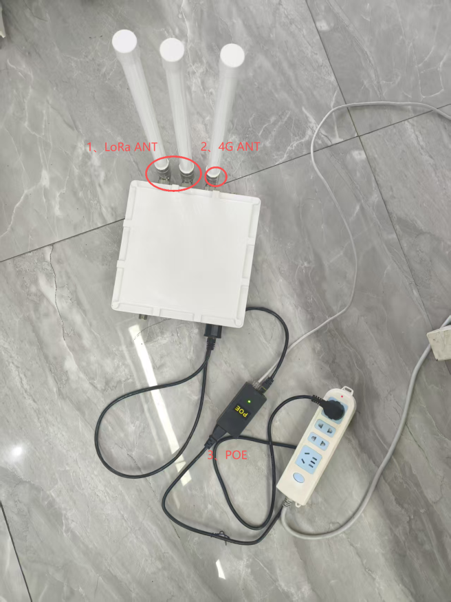
Note the MAC ID on the gateway label; it is required when adding the gateway on the NS platform.
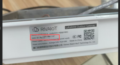
5.1.2 Adding the Gateway on the NS Platform
Log in to the LoRaWAN NS platform (e.g., http://adomodelcloud.com:4560/). The account and password are provided by the account manager.
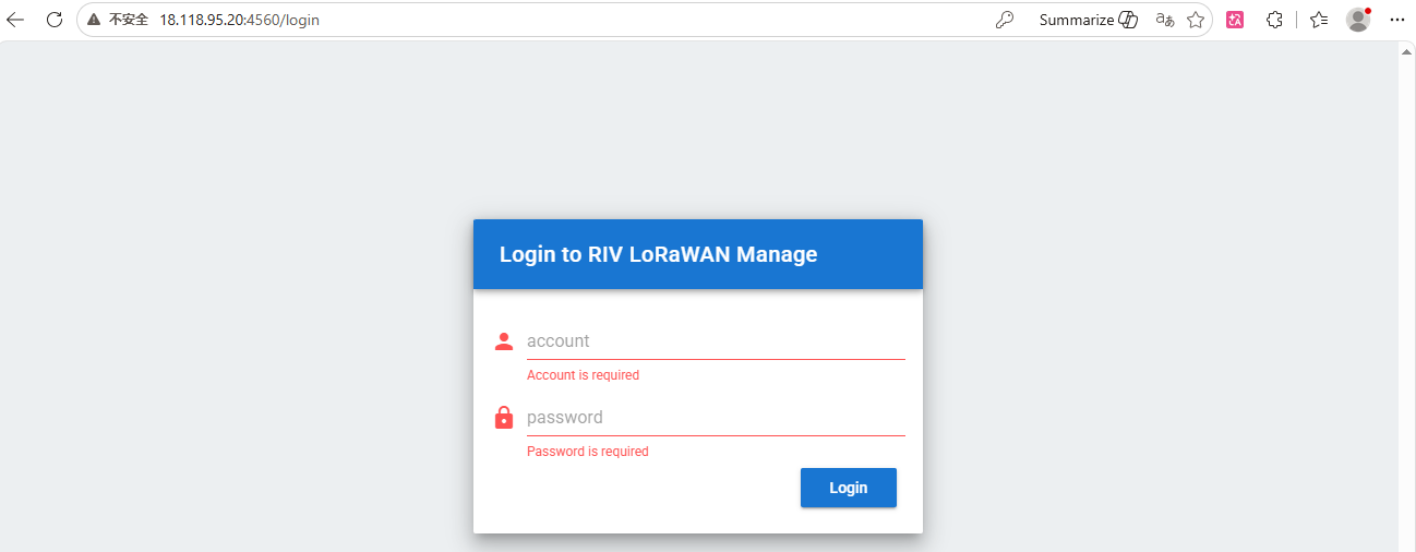
Click the "Gateway" tab on the left and check whether the gateway ID has already been added.
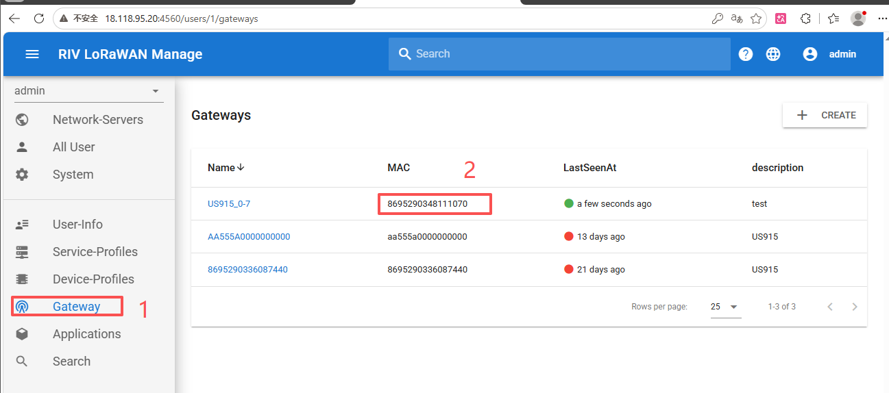
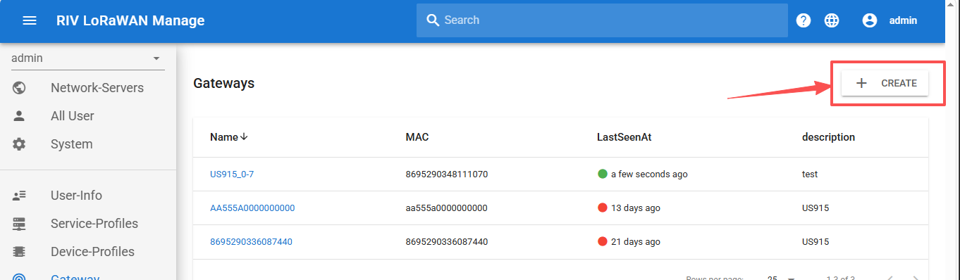
If not, click the "CREATE" button in the upper-left corner to create the gateway.
Enter the gateway ID, select the BAND, and click "CREATE" to finish.
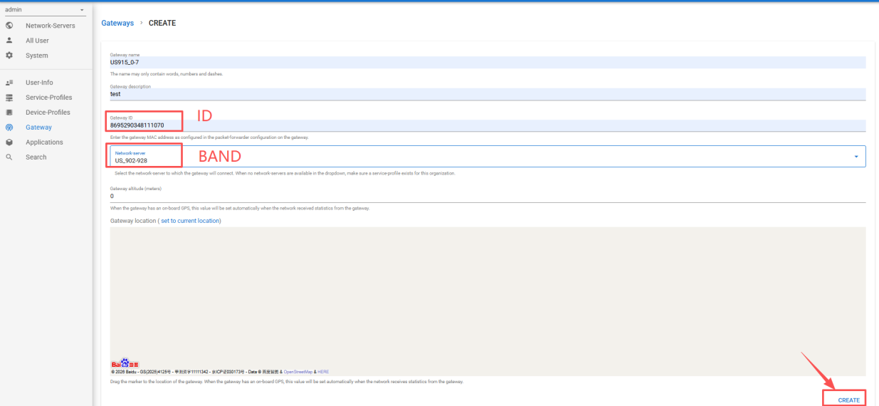
BAND: for North America, select US_902-928 (channels 0-7).
| Region | Band | BAND Parameter | Channels |
|---|---|---|---|
| North America | US915 | US_902-928 | 0~7 |
| North America | US915 | US_902-928_2 | 8~15 |
| Australia | AU915 | AU_915-928 | 0~7 |
5.1.3 Gateway Online Verification
After powering on the gateway, check its status in the Gateway list on the NS platform.

A red dot means the gateway is offline; a green dot means it is online.
With a good network environment, the gateway typically comes online within 1-3 minutes (5 minutes at most).
5.1.4 Troubleshooting: Gateway Cannot Come Online
If the gateway cannot come online, open the gateway configuration page to check whether the parameters are correct. Only access via the management platform is described here; for other methods, refer to the gateway documentation. Steps:
- Log in to the IoT device management platform at http://adomodelcloud.com/ (the account and password are provided by the account manager).
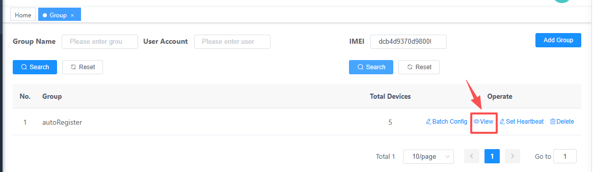
- Click "Device Management" - "Group".
- Enter the gateway ID in the "IMEI" field and click "Search".
NoteIf the search fails, enter the gateway admin page via Wi-Fi or another method as described in the gateway manual.
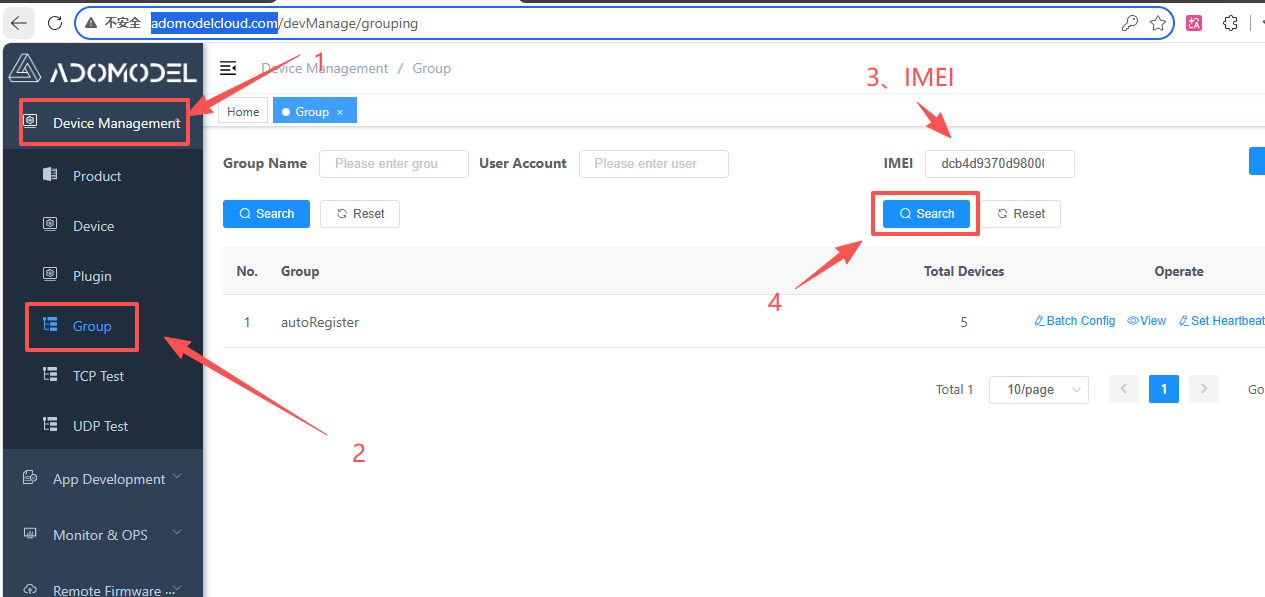
- Click "View" for the found gateway.
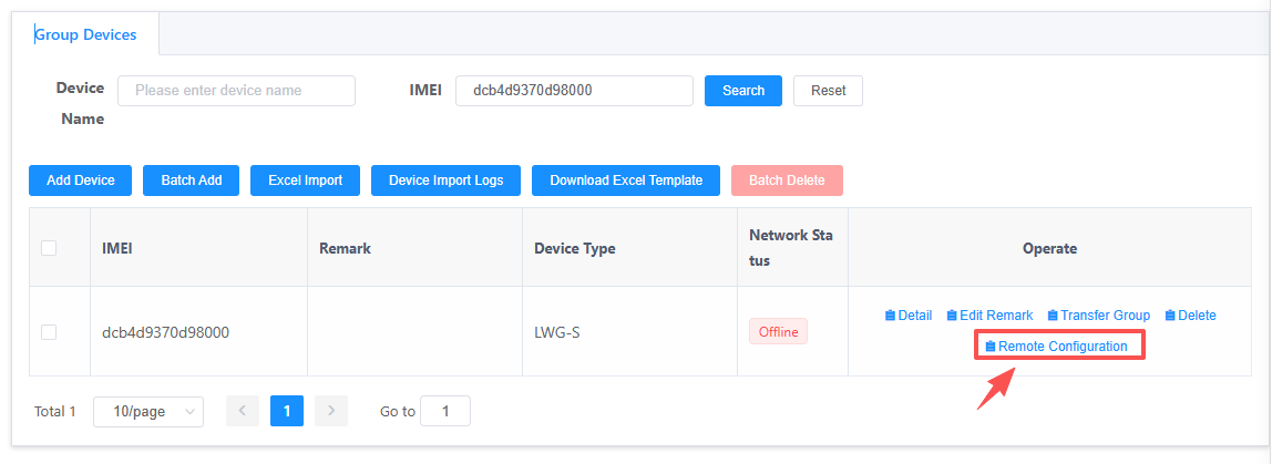
- Click "Remote Configuration".
- Remote configuration is available only when the gateway is in the Online state.
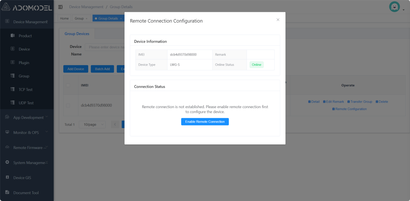
First click Enable Remote Connection.
- Click Open Configuration Page.
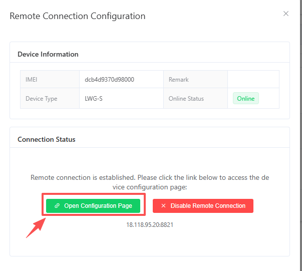
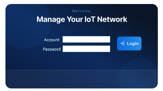
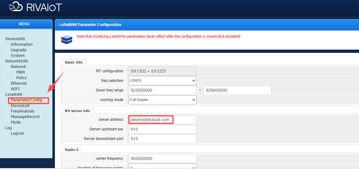
- Log in to the gateway admin page (default account root, password admin) and verify that the NS server address and channel configuration are correct.
5.2 Adding the F Module Device Node on the NS Platform
5.2.1 Creating an Application
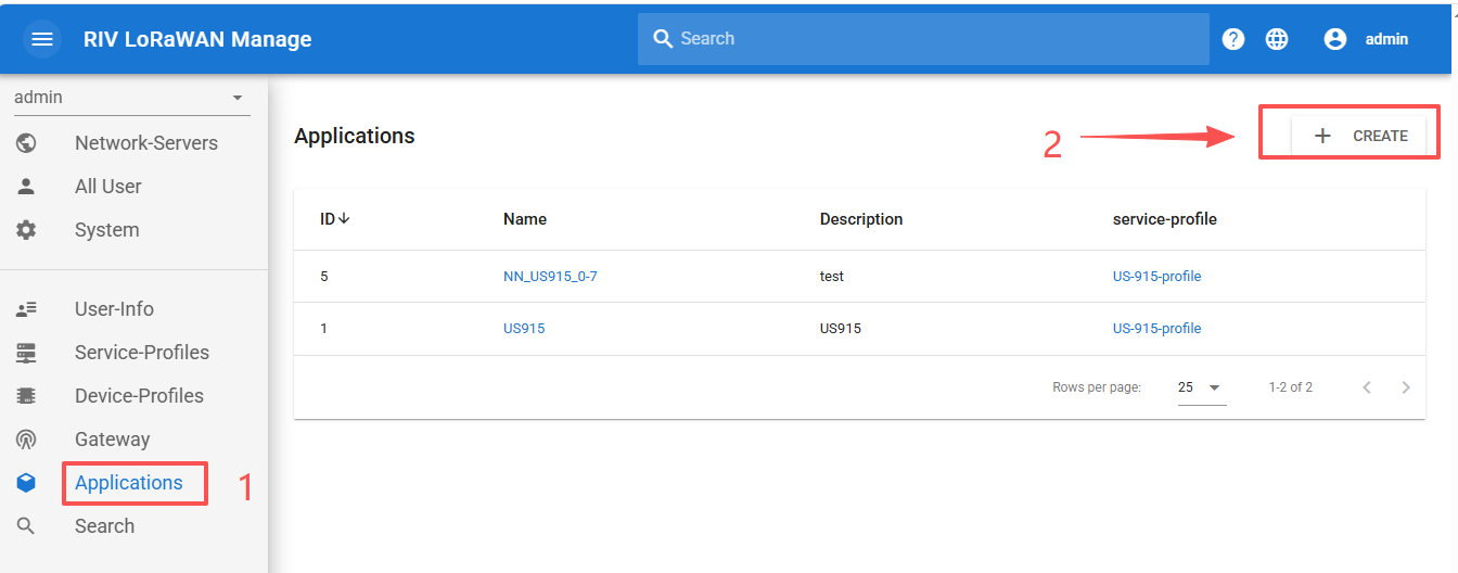
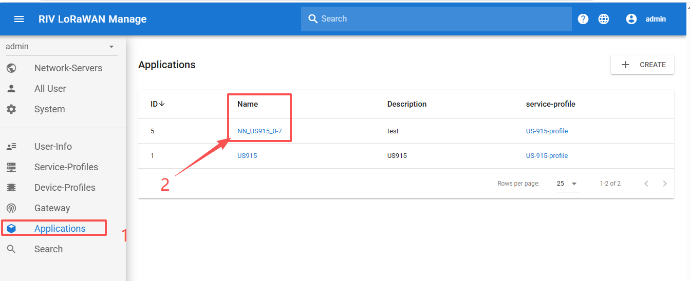
On the NS platform, click "Application" on the left, then "CREATE" in the upper-right corner to create a new application.
Enter the application name and description, select the Service-profile (e.g., US-915-profile for North America US915), and click Create.
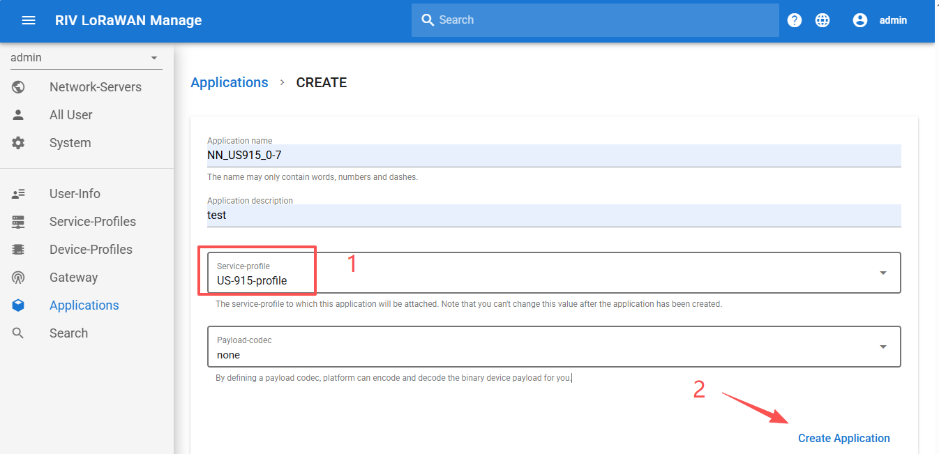
| Region | Band | Service-profile | Channels |
|---|---|---|---|
| North America | US915 | US-915-profile | 0~7 |
| North America | US915 | US-915-2-profile | 8~15 |
| Australia | AU915 | AU915 | 0~7 |
5.2.2 Adding a Device Node
Click the application name to open it, then click "CREATE" in the upper-right corner to create a new node.
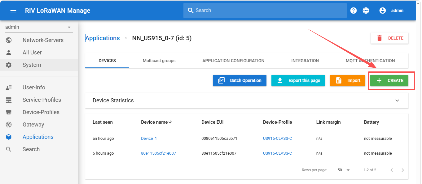
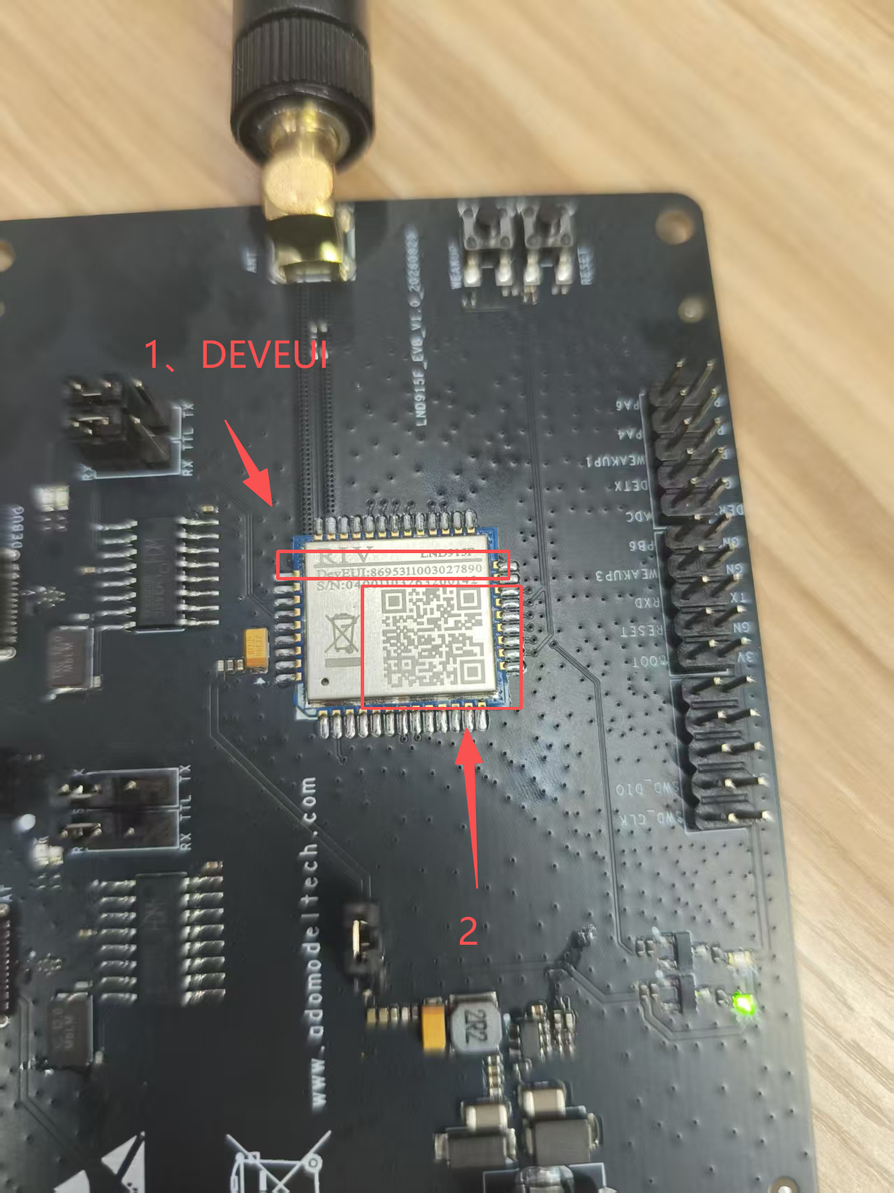
Fill in the Device EUI (DEVEUI): it can be read from the chip silkscreen or the QR code on the development board, or queried with an AT command (see Chapter 6).
Select the Device-profile according to test requirements; Class A is recommended for simplicity.
| Operating Mode | Activation | Device-profile Option |
|---|---|---|
| Class A | OTAA | US915_OTAA_CLASSA |
| Class C | OTAA | US915-CLASS-C |
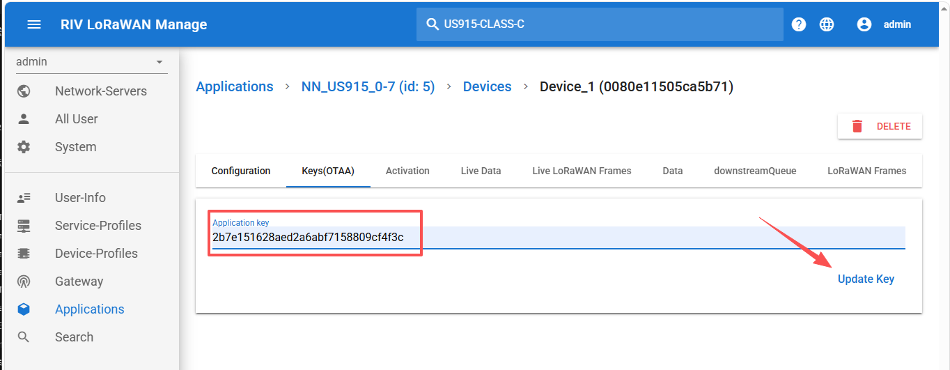
After clicking "CREATE" to create the device, the page jumps to the Keys (OTAA) page.
Enter the Application key (APPKEY): scan the QR code on the chip or query it with an AT command.
Click "Update Key" in the lower-right corner to update the key.
6. F Module AT Command Configuration
After the NS platform is configured, use AT commands to configure the F module so that its parameters match the NS platform.
Wire the development board as follows.
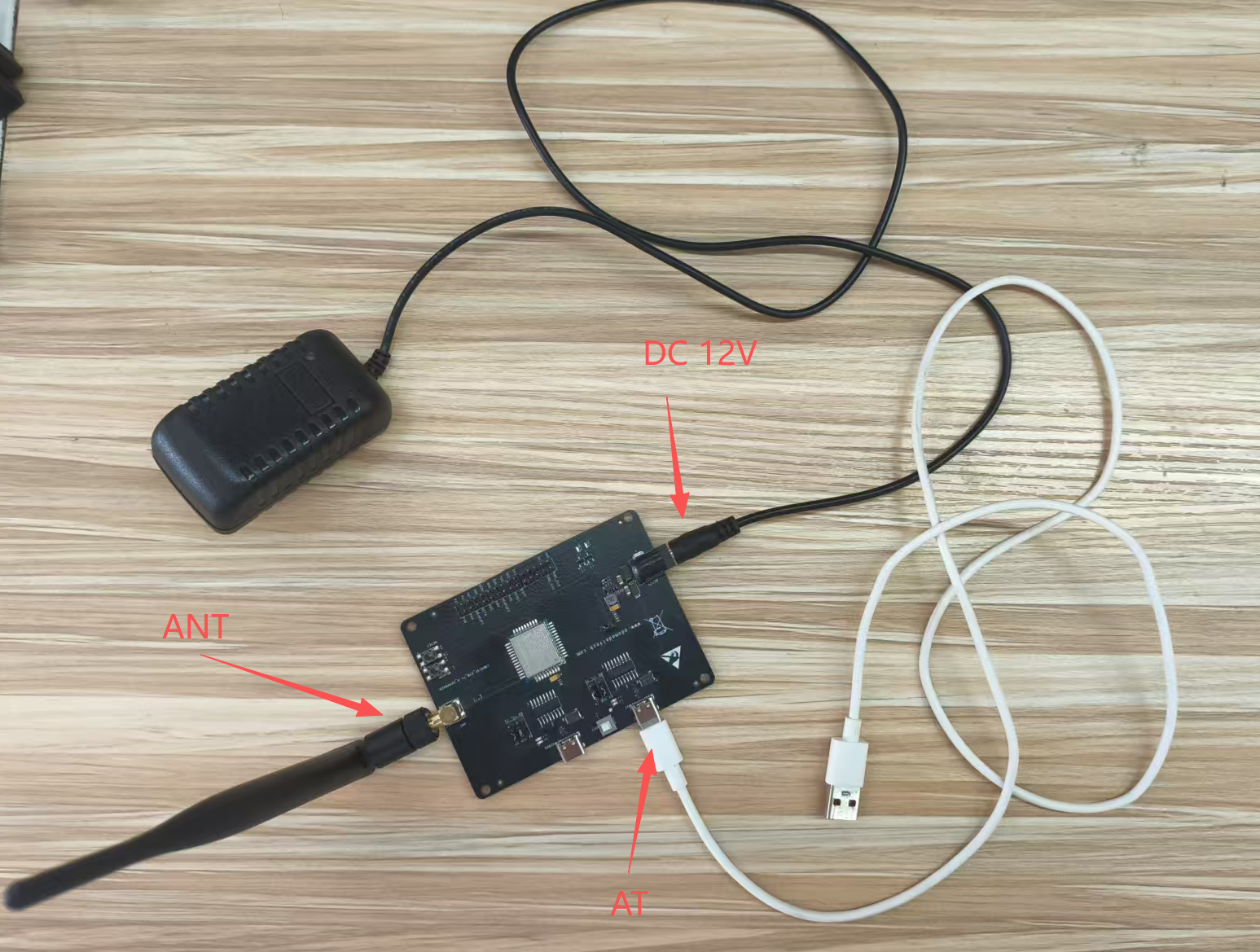
6.1 Serial Connection and Parameter Settings
Connect the module's AT port to the PC via USB and open a serial terminal tool on the PC.
Serial port parameters:
| Parameter | Setting |
|---|---|
| Baud rate | 9600 |
| Data bits | 8 bit |
| Stop bits | 1 bit |
| Parity | None |
| Terminator | Carriage return + line feed (CR+LF, i.e., \r\n) |
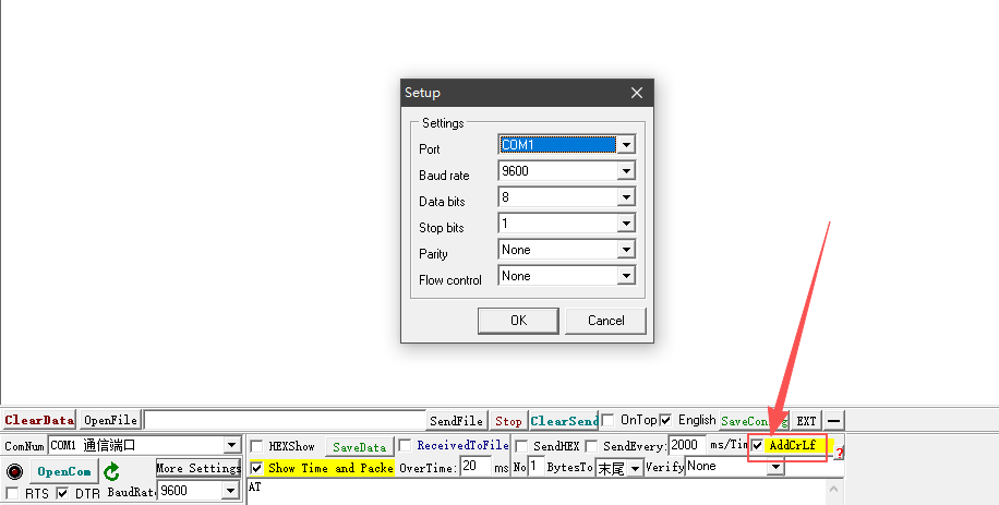
6.2 Serial Connection Verification
After power-on, send an AT command on the AT port to verify that serial communication is normal:
Send: AT
Receive: OK
An OK response means the serial connection is normal. If there is no response, check the serial wiring, the jumper cap configuration, and the baud rate.
6.3 Frequency Band (AT+BAND)
Set the F module's operating band. It must match the band configured on the gateway and the NS platform.
Query the current band:
Send: AT+BAND=?
Receive: 8:US915
OKQuery the list of available bands:
Send: AT+BAND?
Receive: 0:AS923
1:AU915
2:CN470
3:CN779
4:EU433
5:EU868
6:KR920
7:IN865
8:US915
9:RU864
...
OK
Set the band (US915 is No. 8 and is configured by default):
Send: AT+SAVE=0
Receive: RESET
Send: AT+BAND=8
Receive: OK
Send: AT+SAVE=1
Receive: OK
6.4 Join Parameter Configuration
6.4.1 Setting the DEVEUI (AT+DEVEUI)
The DEVEUI is the device's unique identifier and must match the Device EUI entered when adding the device on the NS platform.
Query:
Send: AT+DEVEUI=?
Receive: +DEVEUI:0e8044007b446033
OKSend: AT+SAVE=0
Receive: RESET
Send: AT+DEVEUI=0e8044007b446033
Receive: OK
Send: AT+SAVE=1
Receive: OK6.4.2 Setting the APPKEY (AT+APPKEY)
The APPKEY is the application key — 32 hexadecimal characters (128-bit) — and must exactly match the Application key entered on the NS platform.
Send: AT+APPKEY=?
Receive: +APPKEY:2b7e151628aed2a6abf7158809cf4f3c
OKSend: AT+SAVE=0
Receive: RESET
Send: AT+APPKEY=2b7e151628aed2a6abf7158809cf4f3c
Receive: OK
Send: AT+SAVE=1
Receive: OK6.5 Join Mode Setting (AT+NJM)
Set the module's join mode. OTAA (Over-The-Air Activation) is recommended.
| Value | Join Mode | Description |
|---|---|---|
| 0 | ABP | Activation By Personalization; communicates directly with pre-provisioned keys |
| 1 | OTAA | Over-The-Air Activation; joins over the air (recommended) |
Send: AT+NJM=?
Receive: +NJM:OTAA
OKSend: AT+SAVE=0
Receive: RESET
Send: AT+NJM=1
Receive: OK
Send: AT+SAVE=1
Receive: OK7. Join Test
7.1 Prerequisites for Joining
Before joining, confirm that the following conditions are met:
- The gateway is powered on and shown online (green dot) on the NS platform.
- An application has been created and the device node added on the NS platform.
- The F module is in OTAA mode, and its BAND, DEVEUI, and APPKEY all match the NS platform.
- The antenna is firmly connected to the F module's ANT RF connector.
7.2 OTAA Join Operation (AT+JOIN)
Send the join command; the module will initiate an OTAA join request:
Send: AT+JOIN
Receive: OKJoin success:
Receive: JOINEDJoin failure:
Receive: +CMEE ERROR:200- If joining fails repeatedly, first check the parameter matching per the prerequisites in 7.1.
- After more than 10 consecutive join failures, the module stops joining. Send
AT+RESETor power-cycle the module.Send: AT+RESET Receive: RESET - If all parameters are correct but joining still fails, adjust the join window and retry. Recommended range: 4950-5050 (prefer 5000).
Send: AT+RXDELAY=1,5000 Receive: OK Send: AT+JOIN Receive: OK - Wait about 8 seconds.
Receive: JOINED
Command description:
| Command | Function | Description |
|---|---|---|
AT+JOIN | Initiate joining | The module sends a Join Request and waits for the NS to return a Join Accept |
AT+JOIN? | Query join status | Returns whether the module has joined (0 = not joined, 1 = joined) |
AT+JOIN=1 | Clear join status | Clears the current join status and returns the module to the not-joined state |
Join status query:
Send: AT+JOIN?
Not joined:
Receive: +JOIN:0
OK
Joined:
Receive: +JOIN:1
OK
7.3 Join Verification
7.3.1 Serial Port Verification
After a successful join, the AT port returns the "JOINED" message. The join status can also be queried with AT+JOIN=?.
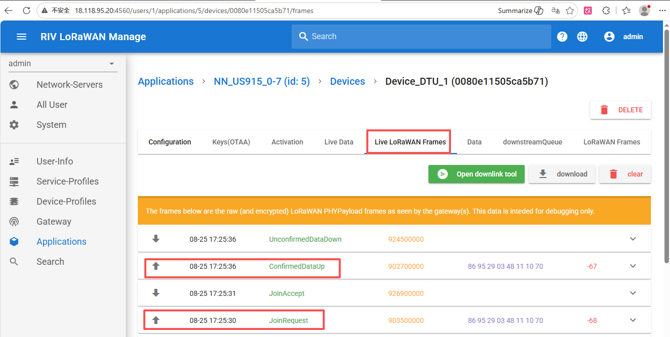
7.3.2 NS Platform Verification
On the NS platform, open the application and click the device node.
Click the "Live LoRaWAN Frame" tab.
Power-cycle the F module or send AT+JOIN; the join frames can then be seen, including "JoinRequest" (join request) and "JoinAccept" (join accept).
Uplink data is indicated by "Up".
8. Uplink Test
The uplink test verifies that the F module can send data to the NS platform via AT commands. Prerequisite: the F module has successfully joined.
8.1 Downlink Echo Configuration (AT+DPDATA)
Before uplink/downlink testing, it is recommended to enable downlink data display so that downlink data can be observed:
Send: AT+DPDATA=1   // Enable downlink data display
Receive: OK| Value | Function | Description |
|---|---|---|
| 0 | Disable downlink echo | Disables downlink data display |
| 1 | Enable downlink echo | Downlink data is printed automatically when received |
| 2 | Enable downlink cache | Caches downlink data inside the module |
| 3 | Retrieve cached data | Retrieves one downlink data record from the cache |
| 4 | Clear cache | Clears all cached downlink data |
8.2 HEX-Mode Uplink Test (AT+SEND)
In HEX mode, data is sent in hexadecimal format and the data length must be specified.
Command format: AT+SEND=<Fport>,<len>,<appdata>
| Parameter | Description | Range |
|---|---|---|
| <Fport> | Uplink port number | 1~223 |
| <len> | Data length | >0: HEX mode, value is the data length (1-223); 0: String mode |
| <appdata> | Data content | In HEX mode, hexadecimal data with an even number of digits |
HEX-mode send example:
Send: AT+SEND=1,16,00112233445566778899aabbccddee
Receive: OK
Explanation: port 1, data length 16 bytes, data content 00112233445566778899aabbccddee.
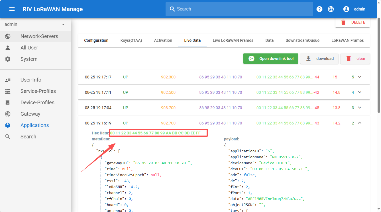
8.3 Viewing Uplink Data on the NS Platform
On the NS platform, open the application and click the device node.
Click the "Live Data" tab.
The uplink data sent by the F module can be viewed.
9. Downlink Test
The downlink test verifies that data sent from the NS platform is correctly received by the F module. Prerequisites: the F module has joined, and at least one uplink has been sent.
9.1 Enable Downlink Data Display
Make sure downlink data display is enabled:
Send: AT+DPDATA=1   // Enable downlink data display
Receive: OK
9.2 Sending Downlink Data from the NS Platform
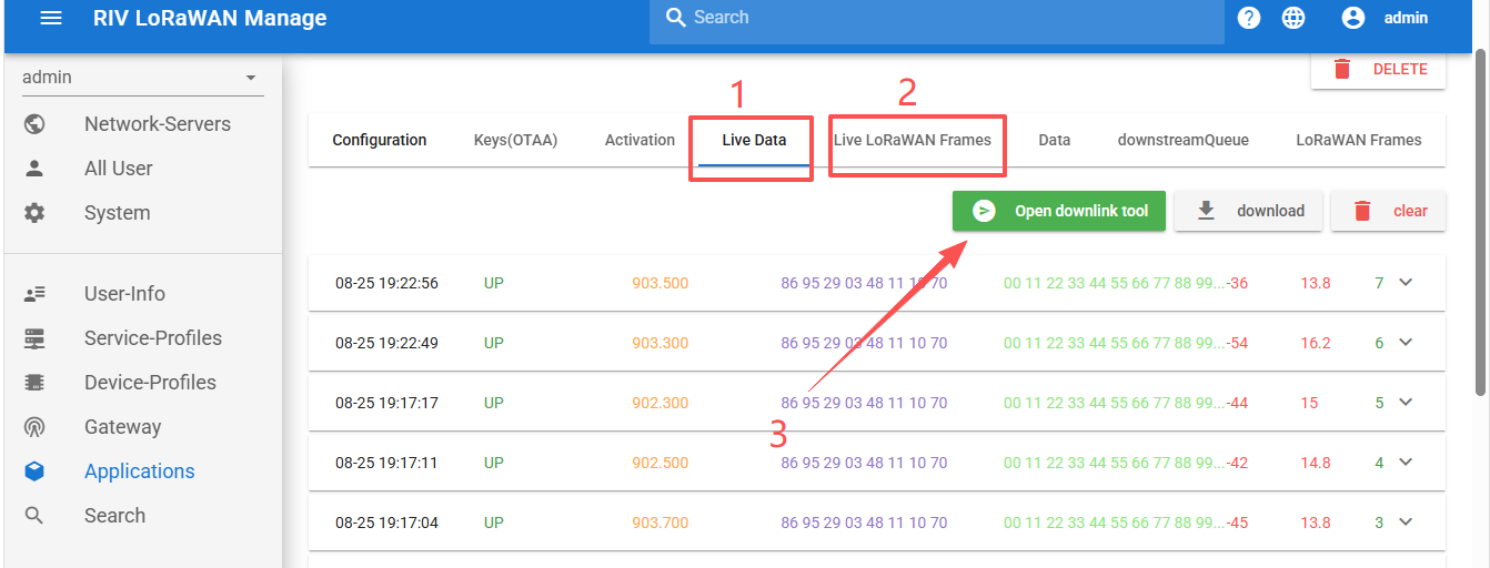
- On the NS platform, open the application and click the device node.
- Click the "Live Data" or "Live LoRaWAN Frames" tab.
- Click "Open downlink tool" to open the downlink tool.
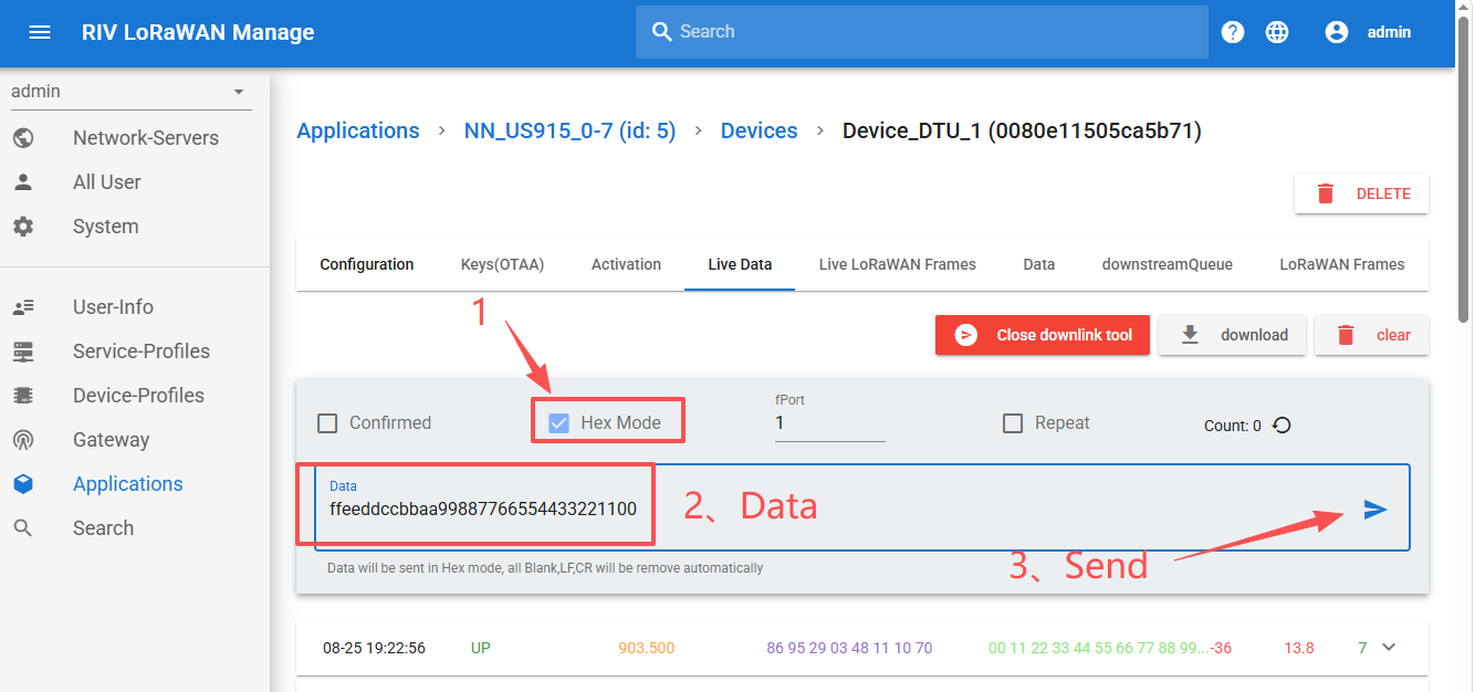
- Check "Hex Mode" (hexadecimal mode).
- Enter any hexadecimal downlink data content.
- Click "Send".
9.3 Downlink Reception Verification
9.3.1 Serial Port Verification
Because the module operates in Class A, one uplink must be sent before a downlink from the NS can be received.
After the NS sends data, send one uplink from the F module:
Send: AT+SEND=1,1,12
Receive: +DPDATA:1,16,ffeeddccbbaa99887766554433221100
Format: +DPDATA:<Fport>,<len>,<data>
| Field | Description | Example |
|---|---|---|
| <Fport> | Downlink port number | 1 |
| <len> | Data length | 16 |
| <data> | Downlink data content (HEX) | ffeeddccbbaa99887766554433221100 |
10. Complete Test Procedure Summary
The following is the complete AT command procedure for F module joining and uplink/downlink testing; execute the steps in order:
Phase 1: Environment setup and configuration
AT   // Verify serial connection
AT+BAND=?   // Verify band (US915)
AT+DEVEUI=?   // Verify DEVEUI
AT+APPKEY=?   // Verify APPKEY
Phase 2: Join test
AT+JOIN   // Initiate join
// Wait for JOINED
AT+JOIN=?   // Query join status
Phase 3: Uplink test
AT+DPDATA=1   // Enable downlink echo
AT+SEND=1,8,0011223344556677   // HEX-mode uplink
Phase 4: Downlink test
AT+DPDATA=1   // Ensure downlink echo is enabled
// Send downlink data from the NS platform with the downlink tool
// The serial port automatically prints: +DPDATA:<port>,<len>,<data>
11. FCC Compliance Information
11.1 FCC Identification
The TK-LND915F evaluation kit integrates the LND915F LoRaWAN module, which has been certified by the FCC as a Single Modular Transmitter under Part 15 Subpart C of the FCC Rules (Part 15 Spread Spectrum Transmitter, frequency range 902.3-914.9 MHz, FCC Rule Part 15C).
This device contains FCC ID: Z5J-REACHLND915.
11.2 Compliance Statement
Note: Changes or modifications not expressly approved by the party responsible for compliance could void the user's authority to operate the equipment.
11.3 RF Exposure and Antenna Requirements
To satisfy FCC RF exposure requirements, the antenna shall be installed and operated with a minimum distance of 20 cm (7.9 inches) from all persons. This device must not be co-located or operated in conjunction with any other antenna or transmitter.
Use only the antenna supplied with this kit. Do not substitute an antenna of higher gain without verifying compliance with the limits authorized by FCC grant Z5J-REACHLND915.
11.4 Usage Restrictions for Integrators
This evaluation kit is intended for development, testing, and prototyping by engineers and developers; it is not a finished consumer product.
Integrators who embed the certified LND915F module into a final product must follow the module manufacturer's integration instructions, and the host product must be verified for compliance with all applicable FCC rules before it is marketed or operated (see KDB Publication 996369 for modular transmitter integration requirements).